

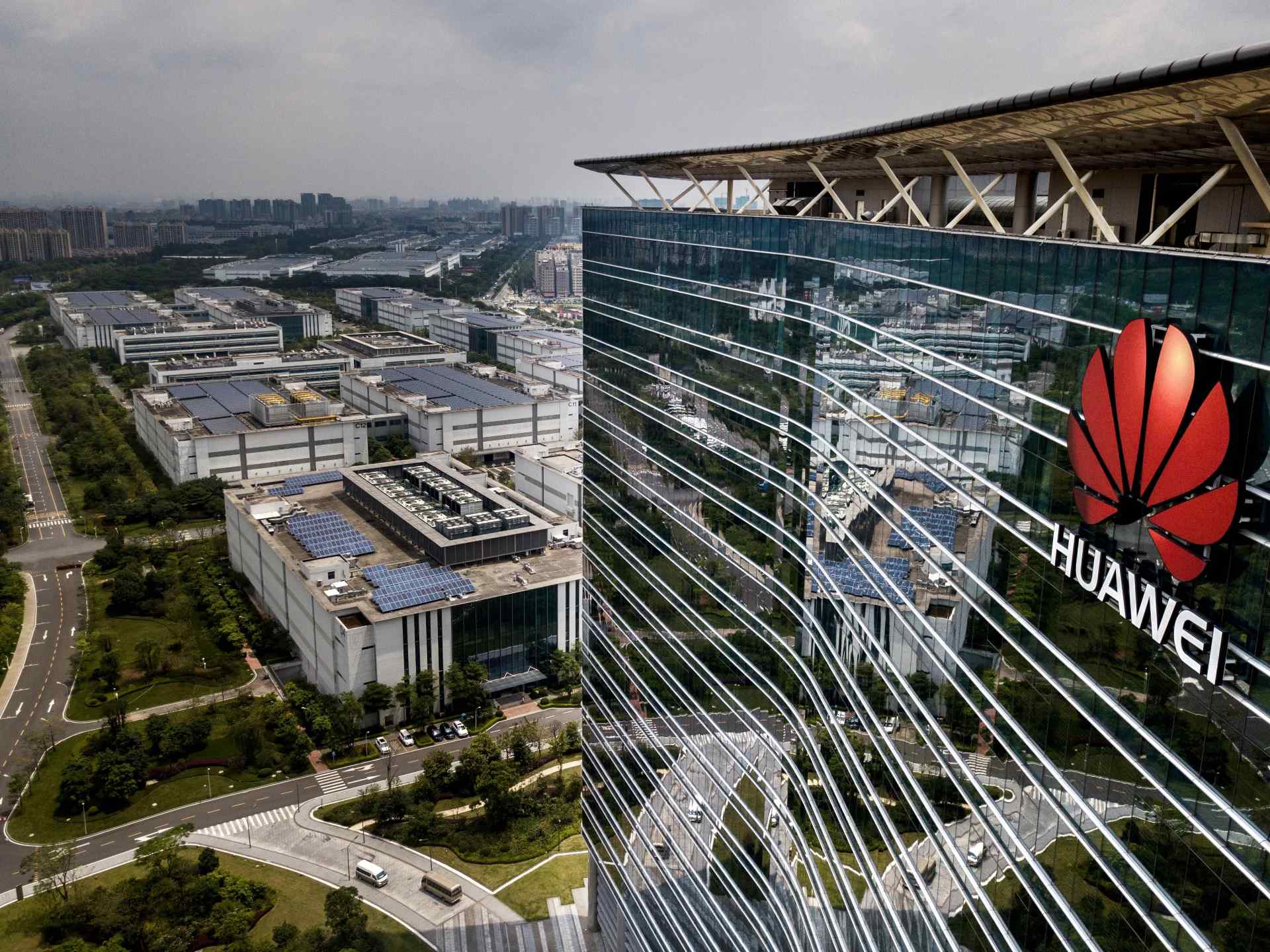
SMIC and Huawei might need efficiently developed the 5nm course of for future chipsets, however there’s a technological ceiling that the Chinese language agency can not part via if it continues to depend on current DUV equipment. With no solution to get its palms on cutting-edge EUV chipmaking instruments from corporations like ASML, a brand new report states that Huawei is taking issues into its personal palms, and that’s by closely investing in an R&D facility with the only real objective of constructing superior equipment just like these produced by main corporations.
When accomplished, Huawei’s superior R&D facility is claimed to cowl an space of 224 soccer fields
The U.S. commerce ban has put Huawei on a path of self-sufficiency, however the highway can be filled with potholes, roadblocks, and different obstacles, to not point out the extraordinary capital that the corporate’s route would require. In accordance with Nikkei, a brand new R&D middle close to Shanghai is being constructed, with the principle purpose being to develop chipmaking instruments that can be aggressive with the machines made by ASML, Canon, and Nikon. At the moment, Huawei’s foundry companions SMIC and Hua Hong are barred from buying instruments that enable them to make chips on the 14nm FinFET and 16nm FinFET processes.
As an alternative, each semiconductor manufacturing corporations can solely get their palms on the 28nm lithography methods, placing them at a extreme drawback compared with the US. The opposite drawback is that 90 % of this market is managed by ASML, which is why Huawei is pursuing this R&D facility growth. To date, the corporate has invested roughly ¥12 billion, or $1.66 billion, and when accomplished, its space can be equal to 224 soccer fields and home over 35,000 workers. Additionally, Huawei is claimed to have supplied enticing wage packages to accumulate high expertise within the discipline of semiconductors.
Nonetheless, no Chinese language firm can recruit U.S. residents with inexperienced card holders, leaving Huawei to rent native expertise. There is no such thing as a telling if the partnership between SMIC and Huawei can be as wholesome when the ability is accomplished, however in the interim, it wants all the assistance it will probably get if it desires to take care of the successful streak on its house turf.
Information Supply: Nikkei


