

Some 2D supplies reminiscent of graphene, silicene (completely different from silicone), black phosphorus, and transition steel dichalcogenides (TMDs) are electrically and mechanically superior to others.
These supplies may give rise to high-speed photodetectors, superior sensors, hi-tech versatile electronics, and photo voltaic cells way more environment friendly than those we use right this moment.
Nonetheless, at present, scientists don’t have the proper method to govern and course of these 2D supplies, and this prevents us from harnessing their potential. Nonetheless, findings from a brand new research reveal an answer to this downside.
A workforce of researchers from Finland’s College of Jyväskylä and Serbia-based College of Novi Unhappy recommend that ultrafast laser processing might help us unlock the potential of 2D supplies.
The benefit of ultrafast laser processing
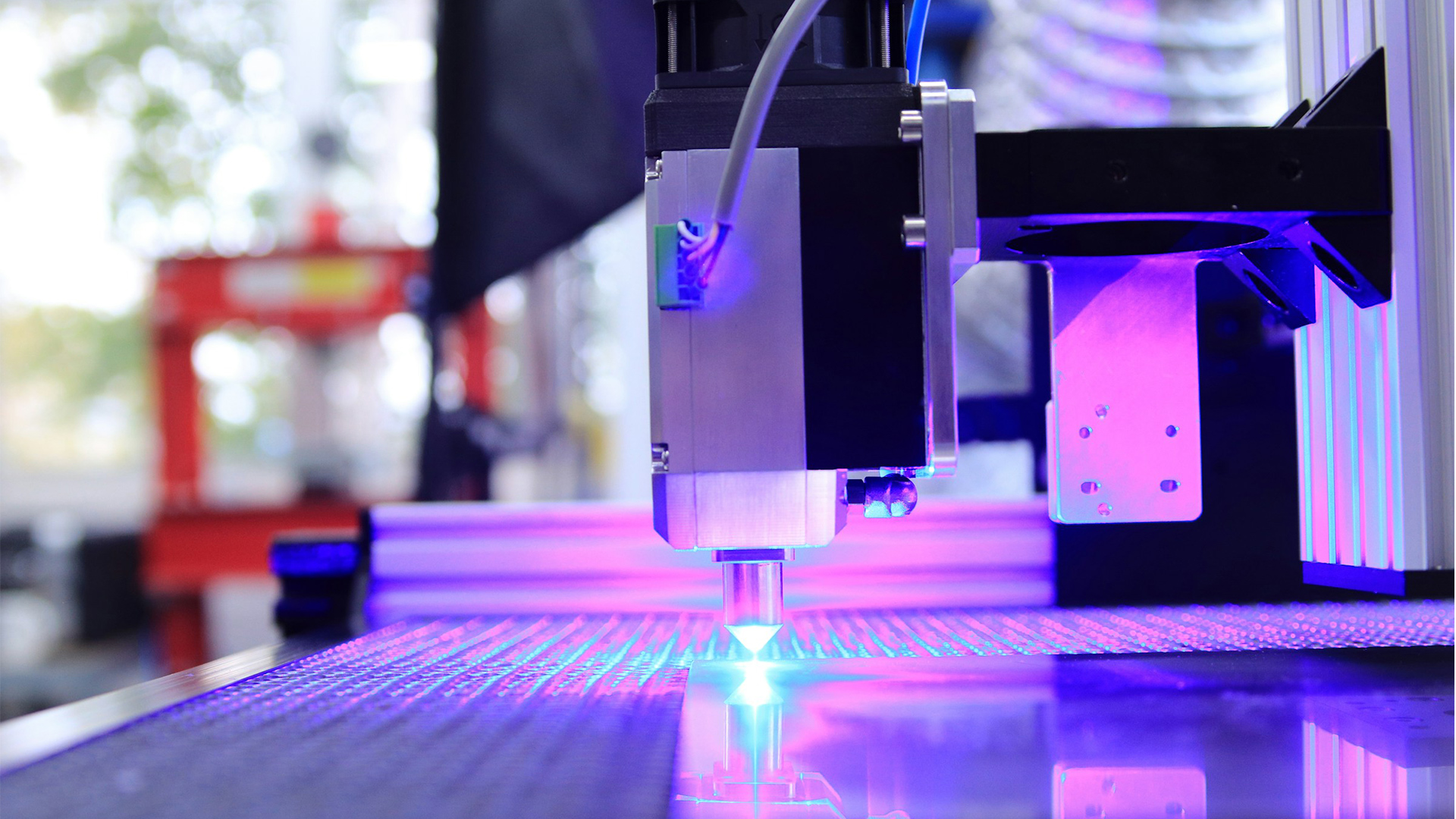
At present, 2D supplies like graphene and TMD are manipulated utilizing continuous-wave (CW) and long-pulsed optical strategies. These strategies contain taking pictures mild beams on 2D materials surfaces to induce change of their bodily and chemical properties.
Nonetheless, each steady wave and long-pulse strategies have one large limitation. When mild strikes a cloth repeatedly within the type of waves or vitality bursts, it ends in the technology of warmth which if not correctly managed can injury the fabric.
That is the place ultrafast laser processing could make an enormous distinction. This system makes use of ultra-short laser pulses to switch supplies with excessive precision and minimal warmth injury.
It will possibly make adjustments in supplies on the nanoscale. “Using the synergetic impact between the vitality states throughout the atomic layers and ultrafast laser irradiation, it’s possible to attain unprecedented resolutions right down to a number of nanometers,” the research authors be aware.
“The flexibility to govern 2D supplies at such a fantastic scale opens up quite a few prospects for the event of novel photonic, digital, and sensor purposes,” they added.
The know-how is but to come back out of the lab
Whereas working on the atomic scale, ultrafast laser processing can successfully allow processes reminiscent of exfoliation (flaking), discount (including electrons to enhance electrical conductivity), and doping (including impurities to switch the properties of a cloth) in a 2D materials.
These processes are essential for altering the bodily and chemical properties of a 2D materials, enabling their use within the improvement of next-generation digital and photonic gadgets.
Nonetheless, ultrafast laser processing is a way which continues to be underneath improvement. Even in lab settings, it includes using costly tools and has a number of challenges associated to optimization and scaling. “This know-how is at present evolving from a laboratory idea to a sensible manufacturing software,” the research authors stated.
Hopefully, additional analysis will make clear methods to make this strategy extra sensible and unveil its different unknown deserves.
The research is revealed within the journal Superior Supplies.
NEWSLETTERThe Blueprint DailyStay up-to-date on engineering, tech, house, and science information with The Blueprint.ABOUT THE EDITORRupendra Brahambhatt Rupendra Brahambhatt is an skilled author, researcher, journalist, and filmmaker. With a B.Sc (Hons.) in Science and PGJMC in Mass Communications, he has been actively working with a few of the most revolutionary manufacturers, information businesses, digital magazines, documentary filmmakers, and nonprofits from completely different elements of the globe. As an creator, he works with a imaginative and prescient to deliver ahead the appropriate data and encourage a constructive mindset among the many plenty.


