

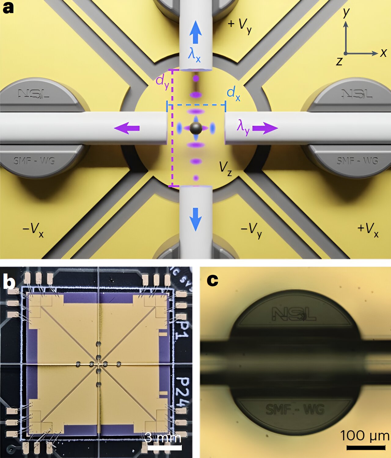
The crew’s on-chip levitation platform. a, The higher optical layer consists of two orthogonal pairs of cleaved single-mode optical fibers. One of many pairs (alongside y) creates a standing wave at λy = 1,550 nm, whereas the second pair (alongside x) creates a standing wave at λx = 1,064 nm. The distances between the fibers are dx = 80 μm and dy = 160 μm. A particle (black) is trapped on the intersection of each standing waves. The sunshine scattered by the particle into the fibers, represented by the arrows, is used for displacement detection. The 4 fibers are positioned above a set of planar electrodes used to use lively suggestions cooling to the charged particle by way of electrical forces: proper and left electrodes for suggestions alongside x, prime and backside for suggestions alongside y, and middle electrode for suggestions alongside z. b, Image of the levitation chip displaying the planar electrodes, 4 optical fibers, fiber mounts near the middle and wire bonds from the chip to the PCB on the corners. c, Optical fiber positioned right into a mechanical mount fabricated by way of two-photon polymerization and used to align and maintain the fibers in place. Credit score:Nature Nanotechnology (2024). DOI: 10.1038/s41565-024-01677-3
The levitation of microscopic objects in vacuum and the management of their actions whereas they’re suspended was first demonstrated a number of a long time in the past. Since then, numerous analysis teams have been engaged on new approaches to regulate levitated objects in vacuum with better levels of freedom.
Whereas most experiments carried out up to now relied on optical methods, some groups have lately began utilizing hybrid experimental platforms that mix ideas rooted in atomic physics. These hybrid platforms allow better management over the movement of levitated objects, unlocking new prospects, similar to drive and torque sensing or precision acceleration.
Researchers at ETH Zurich lately demonstrated the excessive vacuum levitation of a silica nanoparticle on a hybrid photonic-electric chip. Their proposed experimental platform, outlined in a paper revealed in Nature Nanotechnology, was discovered to allow strong levitation, exact place detection and dynamic management of the nanoparticle in vacuum.
“By isolating from the setting and exactly controlling mesoscopic objects, levitation in vacuum has advanced into a flexible approach that has already benefited various scientific instructions, from drive sensing and thermodynamics to supplies science and chemistry,” Bruno Melo, Marc T. Cuairan and their colleagues wrote of their paper.
“It additionally holds nice promise for advancing the research of quantum mechanics within the unexplored macroscopic regime.”
Regardless of current developments in vacuum levitation and movement management of particles, most beforehand launched experimental strategies depend on complicated methods and/or cumbersome gear. This considerably limits their real-world purposes, making them impractical for the event of latest applied sciences.
Some researchers have thus been making an attempt to miniaturize vacuum levitation platforms utilizing electrostatic and optical traps. The levitation achieved utilizing most of their proposed approaches, nevertheless, was not strong sufficient to be utilized to confined units, similar to cryostats and transportable units.
Melo, Cuairan and his collaborators launched a brand new hybrid photonic-electric platform that permits strong levitation, place detection and dynamic management of a nanoparticle on-chip. In distinction with different platforms, their proposed methodology doesn’t require cumbersome lenses and optical gear.
“We present levitation and movement management in excessive vacuum of a silica nanoparticle on the floor of a hybrid optical–electrostatic chip,” Melo, Cuairan and their colleagues wrote. “By combining fiber-based optical trapping and delicate place detection with chilly damping by planar electrodes, we cool the particle movement to a couple hundred phonons.”
In preliminary exams, the crew’s proposed on-chip vacuum levitation and movement management platform achieved outstanding outcomes, with signal-to-noise ratios and optical displacement detection capabilities akin to these of different approaches that depend on cumbersome optical gear. After they mixed their platform with planar electrodes for lively suggestions cooling, the researchers had been additionally capable of calm down the silica nanoparticle and cut back its movement in 3D
The brand new method for on-chip vacuum levitation and movement management launched by this crew at ETH Zurich might quickly open new alternatives for quantum analysis and know-how growth. Of their subsequent research, Melo, Cuairan and their colleagues plan to proceed bettering their platform, as an illustration, utilizing refractive microlenses to additional improve its detection sensitivity and integrating extra subtle optical components (e.g., fiber cavities).
“We envisage that our totally built-in platform is the place to begin for on-chip units combining built-in photonics and nanophotonics with exactly engineered electrical potentials, enhancing management over the particle movement in the direction of complicated state preparation and read-out,” Melo, Cuairan and their colleagues wrote.
Extra info:
Bruno Melo et al, Vacuum levitation and movement management on chip, Nature Nanotechnology (2024). DOI: 10.1038/s41565-024-01677-3
© 2024 Science X Community
Quotation:
The demonstration of vacuum levitation and movement management on an optical-electrostatic chip (2024, July 2)
retrieved 2 July 2024
from https://phys.org/information/2024-07-vacuum-levitation-motion-optical-electrostatic.html
This doc is topic to copyright. Other than any truthful dealing for the aim of personal research or analysis, no
half could also be reproduced with out the written permission. The content material is supplied for info functions solely.


