

We like datacenter compute engines right here at The Subsequent Platform, however because the identify implies, what we actually like are platforms – how compute, storage, networking, and techniques software program are introduced collectively to create a platform on which to construct purposes.
Some historic context is warranted to place the Blackwell platform from Nvidia into perspective. So get a espresso and brace your self.
Nvidia shifted from being a part provider to being a platform maker in April 2016 with the launch of its homegrown DGX-1 techniques, which had been based mostly on its “Pascal” P100 GPU accelerators and a hybrid dice mesh of NVLink ports that coupled eight GPUs into what amounted to a NUMA shared reminiscence cluster. The very first DGX-1, we had been reminded by Nvidia co-founder and chief govt officer Jense Huang within the opening keynote of the GTC 2024 convention, was autographed by Nvidia’s prime brass and hand delivered – actually – by Huang to Sam Altman, one of many co-founders of a shiny new AI startup referred to as OpenAI, which was based 4 months earlier.
With the “Volta” V100 GPU era, the DGX-1 design launched in Could 2017 stayed roughly the identical, with the value tag of the system – Nvidia used to present out costs, keep in mind? – rising by 15.5 p.c towards a 41.5 p.c enhance in efficiency on FP32 and FP64 CUDA cores by an element of 5.7X enhance on efficiency on half precision FP16 math on this new factor referred to as a tensor core, which yielded a 79.6 p.c enchancment in bang for the buck at that precision. It additionally provided INT8 processing for AI inference.
After which, issues acquired loopy within the AI house and, subsequently, issues needed to get loopy with the Nvidia platform structure.
In Could 2018, Nvidia gussied up the V100 SXM3 with its full 32 GB HBM2 complement relatively than the 16 GB that the V100 SXM2 had, after which grabbed a reminiscence atomic swap that its Nvidia Analysis arm had been messing round with and commercialized it as one thing we now know as NVSwitch. And this was the DGX-2 platform.
Twelve NVSwitch ASICs driving 300 GB/sec reminiscence ports and having a complete of 4.8 TB/sec of bi-directional bandwidth had been used to cross-couple these sixteen V100 GPUs, and a set of six PCI-Categorical 4.0 switches had been used to hyperlink two Intel Xeon SP Platinum processors and eight 100 Gb/sec InfiniBand community interfaces to that GPU compute complicated. The system had 1.5 TB of most important reminiscence and 30 TB of flash reminiscence, all for a shocking $399,000 per node.
However right here’s the factor. Because of the reminiscence and the NVSwitch growth, the DGX-2 greater than doubled efficiency, which AI startups desperately wanted, and that meant Nvidia might truly dilute the value/efficiency of the machine by 28 p.c within the discount and make more cash. Nobody had a greater AI node.
With the “Ampere” GPU era, we acquired the DGX A100 system, which was launched in Could 2020 through the corona virus pandemic, the NVLink 3.0 ports on the Ampere GPUs had their bandwidth doubled as much as 600 GB/sec, and subsequently the six NVSwitch ASICs within the DGX A100 system needed to be aggregated to match the identical 600 GB/sec velocity, which meant slicing the NVLink reminiscence cluster measurement from sixteen again to eight.
The DGX A100 had eight A100 GPUs, a pair of AMD “Rome” Epyc 7002 processors, 1 TB of most important reminiscence, 15 TB of flash and 9 Mellanox ConnectX-6 interfaces – one for administration and eight for the GPUs – with a PCI-Categorical 4.0 swap complicated as soon as once more linking the CPUs and NICs to the GPU complicated. Nvidia had simply completed its $6.9 billion acquisition of InfiniBand and Ethernet interconnect maker Mellanox Applied sciences, and was beginning to create what had been very massive clusters on the time utilizing InfiniBand interconnects to connect a whole bunch and 1000’s of A100 techniques collectively. The unique SuperPOD A100 had 140 DGX A100 techniques, with 1,120 A100 GPUs and 170 HDR InfiniBand switches gluing these DGX A100 nodes along with an combination of 280 TB/sec of combination bi-directional bandwidth and delivering only a tad below 700 petaflops of combination FP16 efficiency for AI workloads.
With the “Hopper” H100 GPU accelerator era launched in March 2022, the floating level precision was minimize in half to FP8, the GPUs acquired extra highly effective and ultimately began getting extra reminiscence, and the “Grace” CG100 Arm server CPU was added to the stack and offered 480 GB of LPDDR5 reminiscence with 512 GB/sec of bandwidth for the GPUs to entry over a 600 GB/sec, coherent NVLink into the Hopper GPU complicated.
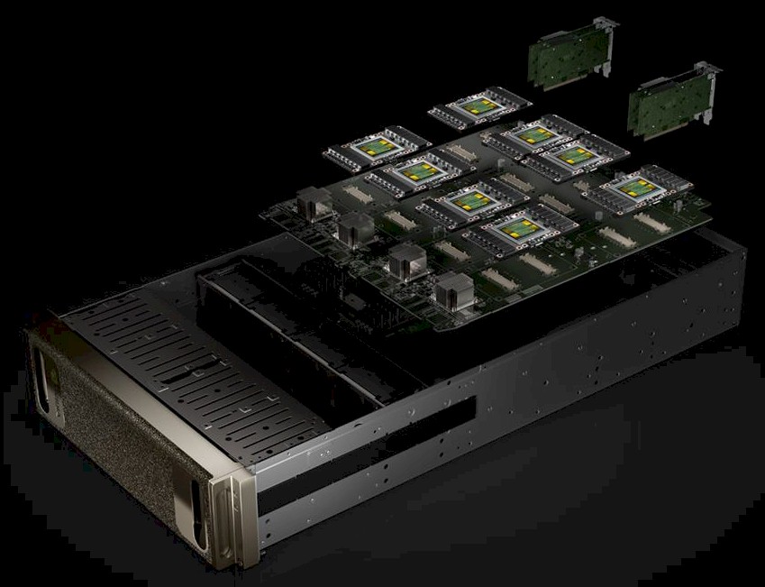
Here’s what the HGX GPU complicated used within the DGX H100 system from Nvidia appears to be like like:
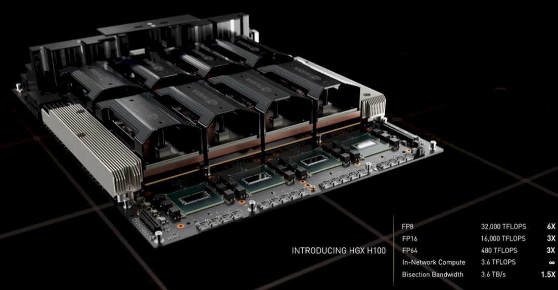
The NVLink 4.0 ports used on the Hopper GPUs delivered 900 GB/sec of bandwidth, and the NVSwitch ASICs needed to be upgraded to supply matching bandwidth throughout a fancy of eight H100 GPUs. This was carried out with 4 dual-chip NVSwitch 3 ASICs, which you’ll see on the entrance of the HGX chassis within the engineering rendering above.
With the NVSwitch 3 ASIC, Nvidia ported the SHARP in-network computing algorithms and circuitry from its InfiniBand switches to the NVSwitch 3 ASIC, giving it the flexibility to do sure collective and discount operations within the community as a substitute of on the DGX node GPUs or ConnextX-7 SmartNICs. Some operations – all scale back, all to all, one to many – naturally belong within the community.
The DHX H100 SuperPOD, which individuals are nonetheless deploying, appears to be like like this:
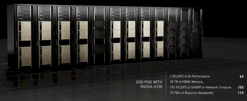
This machine is rated at 1 exaflops at FP8 precision and has 192 teraflops of SHAP in-network processing as effectively. It additionally has 20 TB of HBM3 reminiscence throughout the 256 GPUs within the SuperPOD complicated. For individuals who had been being experimental, there was a approach to used an interconnect comprised of exterior NVSwitch 3 switches to create a shared reminiscence GPU complicated with all of these 256 GPUs in a SuperPOD coherently linked. That NVSwitch interconnected DGX H100 SuperPOD, as we mentioned intimately right here, had 6.4X the dense petaflops of efficiency in comparison with a DGX A100 SuperPOD, however importantly, at 57,600 GB/sec, had 9X the bi-section bandwidth pf that A100 cluster.
Nobody, not even Nvidia, did this full NVSwitch-based DGX H100 SuperPOD in manufacturing, though this has laid the groundwork for the Blackwell techniques.
Which brings us lastly to that Blackwell platform:
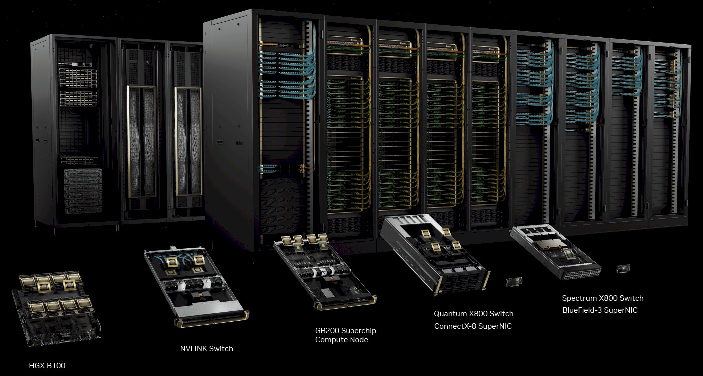
The Blackwell platform begins with the HGX B100 and HGX B200 GPU compute complexes, which will probably be deployed in DGX B100 and DGX B200 techniques and which use geared down variants of the Blackwell GPU that may be air cooled.
The total-on Blackwell GB100 GPU is being saved for the GB200 Grace-Blackwell SuperPOD, which pairs a single Grace CPU to a pair of Blackwell GPUs which can be liquid cooled and utilized in an NVSwitched system referred to as the GB200 NVL72, which because the identify suggests has 72 of the Blackwell GPUs lashed along with an NVSwitch 4 interconnect. This improved interconnect could be scaled to 576 GPUs, which is 2.25X extra “scale out” than was accessible, in idea, on the NVSwitched DGX H100 SuperPOD mentioned two years in the past.
What this implies is a rack with 72 Blackwell GPUs is the brand new unit of efficiency that’s changing an eight-CPU node utilizing H100 or H200 and even B100 or B200 GPUs. Not that you simply won’t be able to purchase these DGX servers and clones of them from OEMs and ODMs that in flip purchase HGX GPU complexes from Nvidia.
Listed below are the feeds and speeds on the HGX B100 and HGX B200 and their B100 and B200 GPUs, that are included within the Nvidia Blackwell Structure Technical Temporary:
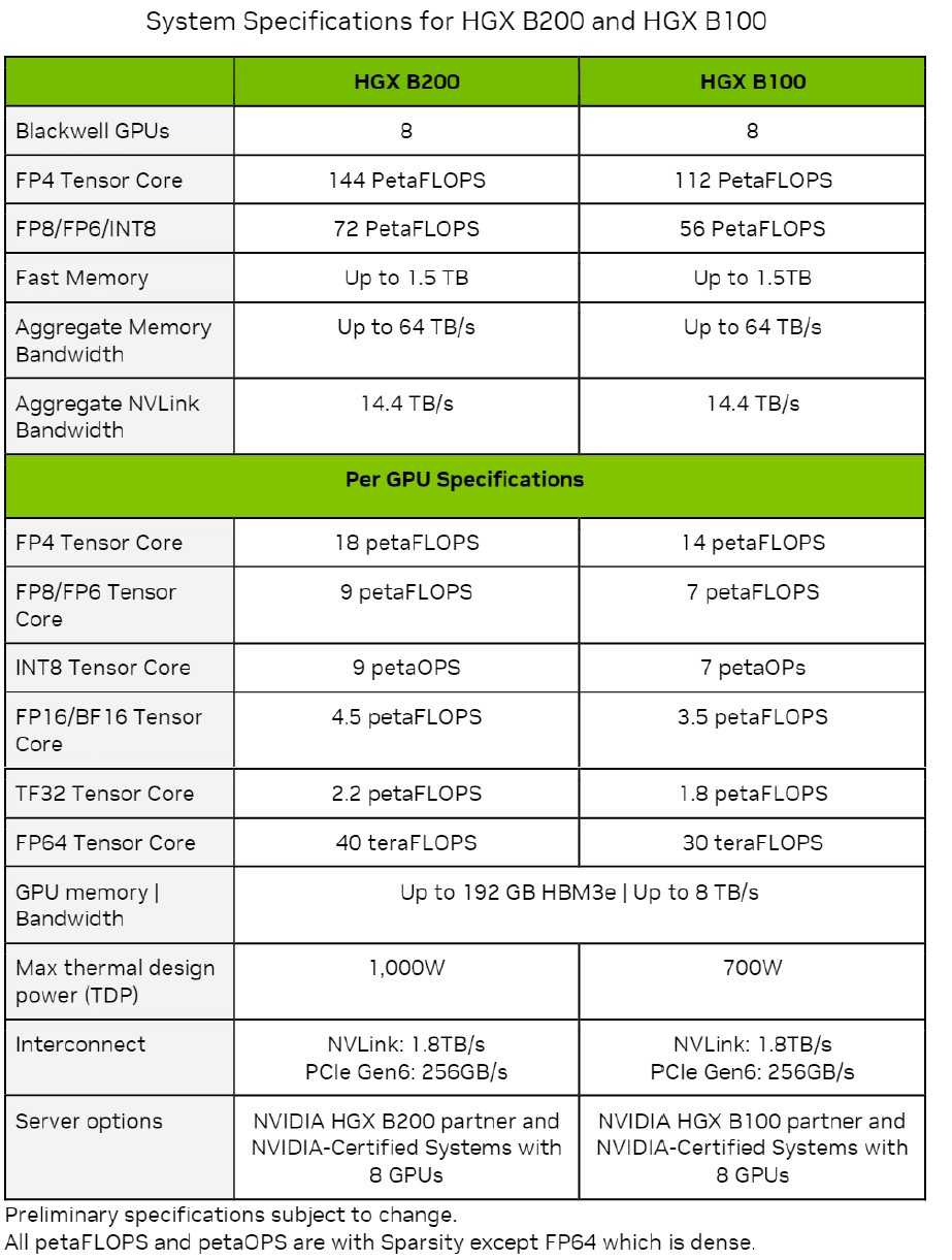
The entire throughput proven on the numerous precisions and knowledge codecs are expressed with sparsity on besides the FP64 throughput, which is proven with sparsity turned off.
What instantly jumps out to us is that each one knowledge is proven operating on tensor cores, not CUDA cores. That doesn’t imply there aren’t any CUDA cores within the Blackwell structure, however it’s odd that they don’t seem to be proven if they’re there – and attention-grabbing if there aren’t any CUDA cores. (Our hunch is that there are none, and we’re sitting in on an architectural briefing later this night to search out out.)
The opposite factor that jumps out is all of these “as much as” caveats within the reminiscence capability and reminiscence bandwidth. Don’t be shocked if the B100 and B200 have lower than the total 192 GB of HBM3E capability and eight TB/sec of bandwidth when these gadgets are bought later this 12 months. If Nvidia can get manufacturing yield and sufficient HBM3E reminiscence, it’s potential. However clearly Nvidia will need to promote the very best bandwidth and highest capability HBM3E on the GB200 techniques that blend the Grace CPU and a pair of Blackwell B200 GPUs that run full-tilt-boogie in a 1,200 watt thermal envelop every and that ship the total 20 petaflops at FP4 precision inherent within the Blackwell two-die GPU complicated, which we talked about right here.
The B100 used within the HGX B100 GPU complexes has the identical thermals because the H100 used within the GHX H100 GPU complexes, so any system that was designed for these Hopper H100 SXM5 GPUs can used the Blackwell B100 SXM6 module, which delivers 14 petaflops at FP4 and seven petaflops at FP8. At FP8 precision, that’s 1.8X extra throughput per Blackwell die in comparison with the Hopper die, and there are two of them, which yields a 3.6X enhance in FP8 efficiency. This strongly suggests to us that there are round 2X extra tensor cores on the Blackwell die than on the Hopper die.
The B200 used within the HGX B200 GPU complicated runs 42.9 p.c hotter and delivers 18 petaflops per two-die socket at FP4 precision. With 9 petaflops at FP8 precision with sparsity on per Blackwell die operating at no matter velocity the B200 is operating at, that’s 2.25X extra oomph than the H100 chip and there are two of them, which yields 4.5X extra efficiency per socket.
Making One Ginormous GPU
One new part in these HGX B100 and HGX B200 techniques is the NVLink 5 port and the NVLink Change 4 ASIC, which the ports on the GPUs speak to. Each have SerDes circuits that run at 100 Gb/sec signaling per lane and with PAM-4 encoding, which carries two bits per sign, that drives the efficient bandwidth to 200 Gb/sec per lane. Lanes are massively aggregated to ship 1.8 TB/sec of bi-directional bandwidth out of the ports on the B100 and B200 GPU complexes and into and throughout the NVLink Change 4 (what we generally simply name NVSwitch 4) ASIC. That NVSwitch 4 ASIC has 7.2 TB/sec of combination bandwidth, which suggests it may possibly drive a complete of 4 1.8 TB/sec NVLink ports. (That’s an unbelievable 72 lanes operating at 200 Gb/sec for every port.)
The SerDes on this ASIC drive 72 ports operating at 200 Gb/sec, and they’re the identical SerDes which can be getting used within the new InfiniBand Quantum-X800 (previously often called Quantum-3), which has 115.2 Tb/sec of combination bandwidth and might drive 144 ports operating at 800 Gb/sec speeds.
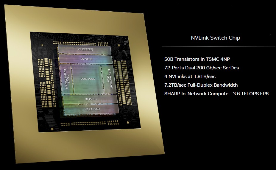
Here’s a zoom in on the NVLink Change 4 die:
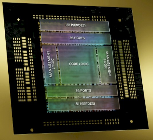
This chip has 50 billion transistors and is applied in the identical TSMC 4NP course of that’s used for the Blackwell GPUs.
The brand new NVLink Change has 3.6 teraflops of SHARP v4 in-network computing for doing collective operations inside the swap, which boosts the effectivity of GPU clusters. Some collective operations which can be carried out in parallel calculations, significantly calculating common weights and delivering them at an middleman stage of a calculation, are greatest carried out within the community, which is at a neighborhood heart of the nodes that it connects to.
Apparently, the NVLink Change 4 ASIC can present a confidential computing area throughout 128 GPUs, and might scale the NVLink coherent reminiscence material throughout a most of 576 GPUs, the latter of which is 2.25X bigger than the 256 CPU theoretical reminiscence material scale with the NVLink Change 3 ASIC. Ian Buck, normal supervisor of hyperscale and HPC at Nvidia, cautions us that identical to that 256 GPU restrict was a theoretical one, meant for analysis not manufacturing, with the NVLink Change 3, that 576 GPU most for NVLink Change 4 can also be meant for analysis, not manufacturing.
Nevertheless, this time round, as expressed within the GB200 NVL72 system that we are going to now stroll by means of, 72 GPUs which can be sharing GPU reminiscence in a good coupling is the brand new unit of compute, like eight or sixteen GPUs have been for the reason that introduction of the DGX line of techniques and their HGX GPU complexes and NVSwitch interconnects. What was as soon as a node is now a full rack. And admittedly, it’s about time.
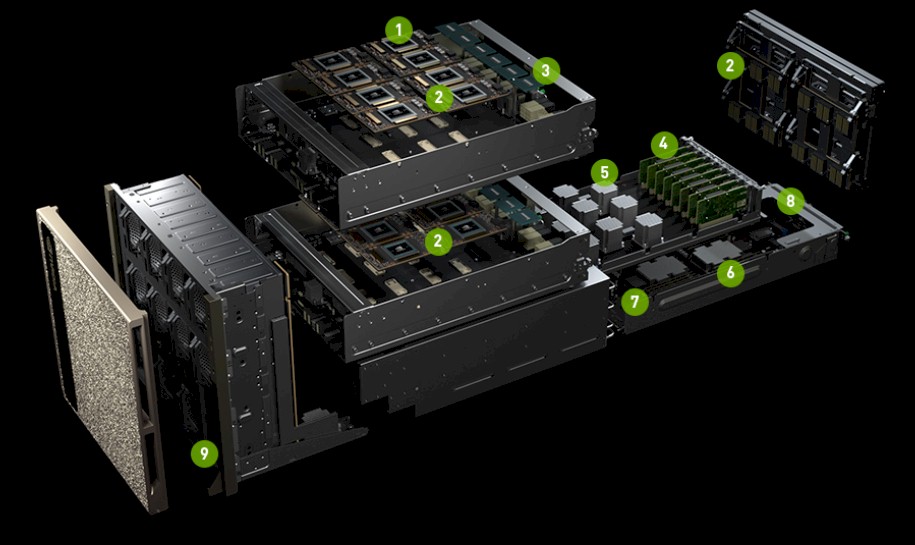
Listed below are the parts within the rack:
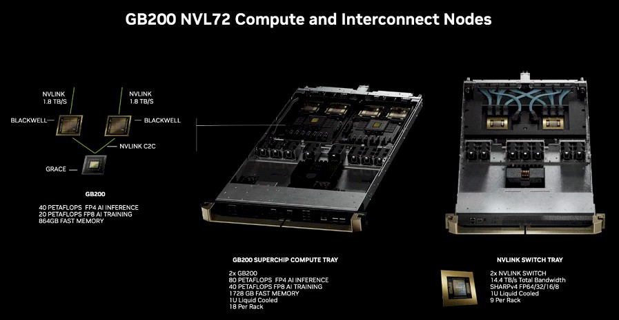
That 2:1 ratio of GPUs to CPUs exhibits that having Grace be so highly effective was not mandatory for AI hosts, and even the adjunct LPDDR5 reminiscence was not wanted as a lot as it’s for the embeddings which can be used for advice engines. Grace solely has a 600 GB/sec NVLink 4.0 port popping out of it, and that is cut up into two, utilizing 300 GB/sec to talk to every Blackwell B200 GPU. That’s much more than PCI-Categorical can do, and in reality, it will likely be early subsequent 12 months earlier than we’ve 256 GB/sec PCI-Categorical 6.0 x16 slots. The 1.8 TB/sec bandwidth that Nvidia will ship this 12 months with NVLink 5.0 ports gained be accessible till round 2032 with PCI-Categorical 9.0 x16 slots delivering 2 TB/sec at the moment.
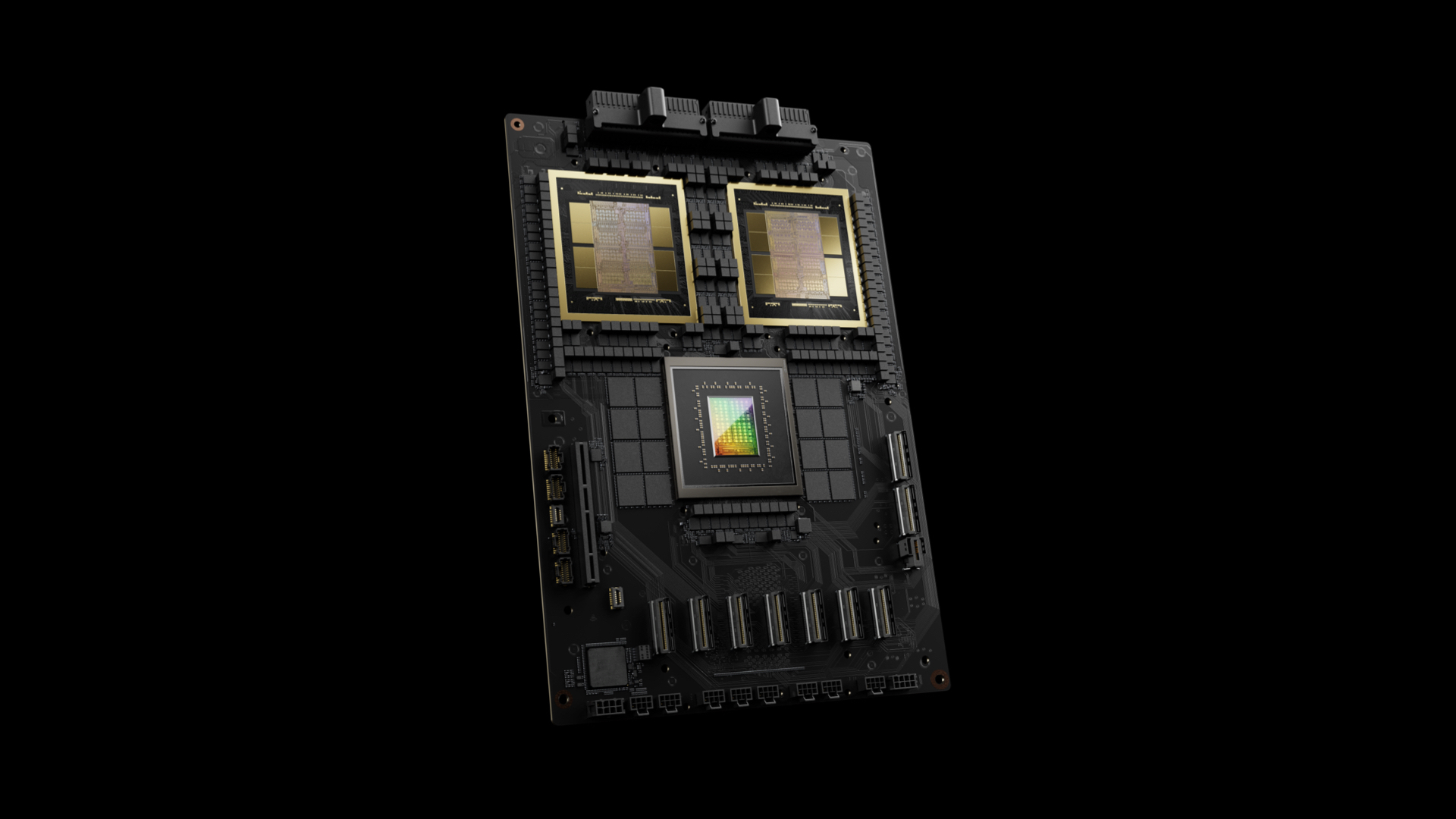
Here’s a zoom on that Grace-Blackwell superchip:
And here’s what the DXG GB200 NVL72 rack system appears to be like like:
The entrance of the rack is on the left and the again of the rack, with miles of copper cable, is on the proper.
This rack is the brand new unit of compute, and the rationale why is straightforward: At these NVLink Change bandwidths, a rack is as far a distance between parts that may nonetheless be interconnected with copper wires and never have to modify to retimers, optical transceivers, and fiber optic cables. Go a lot additional than a rack and you need to transfer into the realm of optics, which provides value and warmth – and a whole lot of each. It’s a suppose we hear many times in system structure.
“So that is what makes it potential,” defined Nvidia co-founder and chief govt officer Jensen Huang as he did a buildup and teardown of the Blackwell rackscale design. “That’s the again, the DGX NVLink backbone, and 130 TB/sec goes to the again of that chassis – that’s greater than the combination bandwidth of the Web, so we will mainly ship every part to everyone inside a second. And so we’ve 5,000 NVLink cables – in complete two miles. Now that is the superb factor. If we had to make use of optics, we might have had to make use of transceivers and retimers, and people transceivers and retimers alone would have value 20,000 watts – 2 kilowatts of simply transceivers alone – simply to drive the NVLink backbone. We did it fully at no cost over NVLink Change and we had been in a position to save the 20 kilowatts for computation. This whole rack is 120 kilowatts, in order that 20 kilowatts makes an enormous distinction.”
And the price of the combination of copper and optical community hyperlinks would elevate the price of the NVLink Change material by an element of 6X, in response to Buck. And that’s the reason, we surmise, that something past 72 GPUs continues to be going to be for analysis, not manufacturing, and that these racks will probably be interlinked with InfiniBand or Ethernet, not NVLink Change, except you may have some huge cash to spare for energy, cooling, and optics.
This rackscale strategy embodied on the top-end of the Blackwell platform was foreshadowed within the “Ceiba” supercomputer being constructed by Nvidia and Amazon Net Companies that we informed you about again in November. That Ceiba machine was based mostly on what is named the DGX GH200 NVL32, and because the identify suggests, it was a rackscale design based mostly on NVLink Change 3 interconnects that related 32 of the Grace-Hopper CPU-GPU superchips collectively right into a shared compute complicated It had 9 NVSwitch techniques to interlink these compute engines and delivered 128 petaflops, 20 TB of complete reminiscence (4.5 TB of that was HBM3E with a complete of 157 TB/sec of combination reminiscence bandwidth), all linked by 57.6 TB/sec of combination NVLink bandwidth.
The Blackwell GB200 NVL72 takes the Ceiba strategy to a complete nuthah degree, as we are saying in New Jersey.
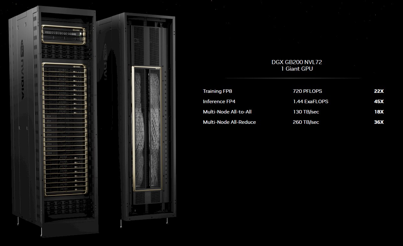
The chart above exhibits the multiples for the GB200 NVL72 in comparison with a DGX H100. However that’s not the true comparability.
The one to check, as Huang walked by means of throughout his keynote, was methods to practice the 1.8 trillion parameter GPT-4 Combination of Consultants LLM from OpenAI. On a cluster of SuperPODs based mostly on the Hopper H100 GPUs utilizing InfiniBand outdoors of the node and NVLink 3 inside the node, it took 8,000 GPUs 90 days and 15 megawatts of juice to finish the coaching run. To do the identical coaching run in the identical 90 days on the GB200 NVL72, it could take solely 2,000 GPUs and 4 megawatts. In case you did it throughout 6,000 Blackwell B200 GPUs, it could take 30 days and 12 megawatts.
This isn’t actually a computation subject as a lot as it’s an I/O and computation subject, Buck defined to us. With these Combination of Knowledgeable modules, there are lots of extra layers of parallelism and communication throughout and inside these layers. There may be the information parallelism – breaking the information set into chunks and dispatching elements of the calculation to every GPU – that’s the hallmark of HPC and early AI computing. Then there may be tensor parallelism (breaking a given calculation matrix throughout a number of tensor cores) and pipeline parallelism (dispatching layers of the neural community processing to particular person GPUs to course of them in parallel to hurry them up). And now we’ve mannequin parallelism as we’ve a mix of consultants who do their coaching and inference so we will see which one is the most effective at giving this sort of reply.
It hurts to consider it, and also you want an AI to maintain monitor of all of it most likely. . . . Buck says that to determine the proper configurations of parallelism to run GPT-4 coaching on the GB200 NVL72 cluster, Nvidia did greater than 2,600 experiments to determine the proper approach to create the {hardware} and cube and slice the mannequin to make it run as effectively as potential. Listed below are a few of these experiments, plotted out:
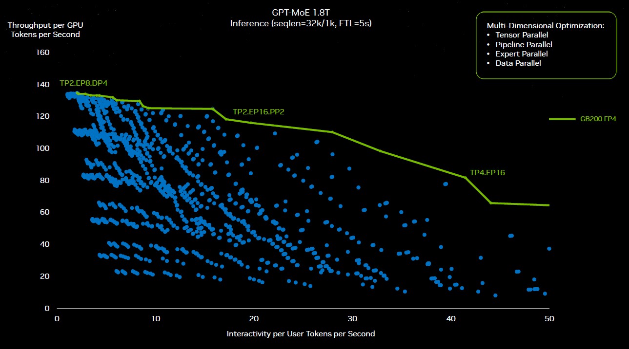
“All these blue dots got here from some repartitioning of the software program,” defined Huang in his keynote. “Some optimizing resolution has to go and work out whether or not to make use of tensor parallel, skilled parallel, pipeline parallel, or knowledge parallel and distribute this monumental mannequin throughout all these completely different GPUs to get the sustained efficiency that you simply want. This exploration house could be unimaginable if not for the programmability of Nvidia’s GPUs. And so we might, due to CUDA, as a result of we’ve such a wealthy ecosystem, we will discover this universe and discover that inexperienced roofline.”
Now, right here is how the Hopper and the Blackwell rooflines look engaged on GPT-4 MOE at 1.8 trillion parameters, and only for enjoyable, there’s a theoretical Blackwell line in purple within the center that exhibits how Blackwell would have carried out if it was simply put collectively in a cluster mixing NVLink Change 3 and 400 Gb/sec InfiniBand because the Hopper techniques had been carried out and caught with FP8 precision and didn’t transfer to the brand new Transformer Engine and FP4 processing for inference. A form of easy silicon improve however not a system improve:
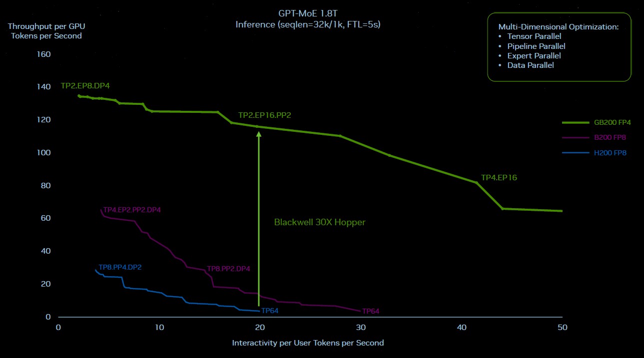
Clearly, simply doing a tough improve to Hopper to make Blackwell was not the reply. And all the issues that enhance inference efficiency by 30X and scale back inference energy consumption by 25X, as Nvidia is claiming, had been the proper strikes.
There are a whole lot of simultaneous results at work right here. Operating this GPT-4 MOE mannequin on a cluster of solely sixteen Hopper-class GPUs – two HGX boards interlinked with InfiniBand – due to the collective operations throughout the degrees of parallelism, about 60 p.c of the wall time for the machine was utilized in communication and solely 40 p.c was solely used for compute. The quicker and fatter NVLink Change interconnect is permitting extra of that compute for use.
With the NVLink Change interconnect throughout 72 GPUs, these GPUs can speak extremely quick to one another – and so they can all speak to one another on the similar time when mandatory and full that chatter quick. Not solely that, there are two GPUs in every node GB200 node, as a substitute of just one GPU per node with the GH200 node. There may be roughly twice as a lot HBM3E reminiscence per GPU and virtually twice as a lot bandwidth. Within the liquid cooled GB200 NVL72 configuration, these two Blackwell sockets have 40 petaflops of FP4 oomph, in comparison with 4 petaflops of FP8 oomph for the one Hopper socket.
The networking is clearly as essential because the compute.
Eight of those GB200 72NVL racks now comprise a SuperPOD, by the best way, and you’ll interconnect them with 800 Gb/sec InfiniBand or Ethernet or go experimental and hyperlink all the 576 GPUs in that half row of racks to create a a lot bigger shared reminiscence system. The latter will most likely have a networking invoice that’s virtually as large because the compute invoice. However, with a 576-GPU reminiscence and compute area, it may be price it. . . . Some years therefore, the row would be the new node, in spite of everything. Like two years from now, based mostly on present developments. And shortly after that, the datacenter would be the new node.


