

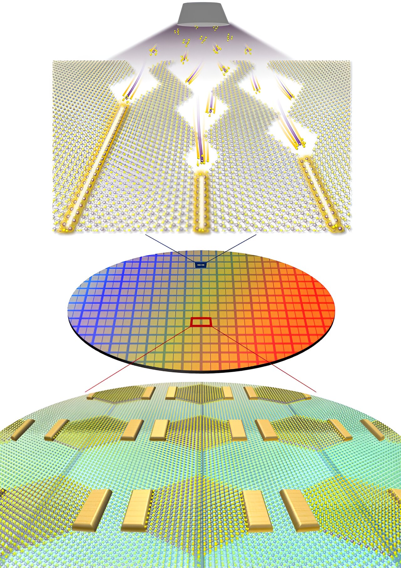
This determine depicts the synthesis of metallic 1D mirror twin boundaries by Van der Waals epitaxial development (prime) and the large-area 2D semiconductor built-in circuit constructed based mostly on these boundaries (backside). By controlling the crystal construction of molybdenum disulfide on the atomic stage utilizing Van der Waals epitaxial development, metallic 1D mirror twin boundaries have been freely synthesized in desired places on a big scale. These boundaries have been utilized as gate electrodes to implement ultra-miniaturized 2D semiconductor transistors with channel lengths on the atomic scale. Credit score: Institute for Fundamental Science
A analysis group led by Director Jo Moon-Ho of the Middle for Van der Waals Quantum Solids inside the Institute for Fundamental Science (IBS) has carried out a novel technique to realize epitaxial development of 1D metallic supplies with a width of lower than 1 nm. The group utilized this course of to develop a brand new construction for 2D semiconductor logic circuits. Notably, they used the 1D metals as a gate electrode of the ultra-miniaturized transistor.
This analysis seems in Nature Nanotechnology.
Built-in units based mostly on two-dimensional (2D) semiconductors, which exhibit glorious properties even on the final restrict of fabric thickness right down to the atomic scale, are a significant focus of primary and utilized analysis worldwide. Nonetheless, realizing such ultra-miniaturized transistor units that may management the electron motion inside a number of nanometers, not to mention growing the manufacturing course of for these built-in circuits, has been met with important technical challenges.
The diploma of integration in semiconductor units is set by the width and management effectivity of the gate electrode, which controls the movement of electrons within the transistor. In standard semiconductor fabrication processes, lowering the gate size under a number of nanometers is inconceivable as a result of limitations of lithography decision.
To resolve this technical downside, the analysis group leveraged the truth that the mirror twin boundary (MTB) of molybdenum disulfide (MoS2), a 2D semiconductor, is a 1D metallic with a width of solely 0.4 nm. They used this as a gate electrode to beat the constraints of the lithography course of.
This determine exhibits an optical microscope picture of the built-in circuit based mostly on 1D mirror twin boundary gates (left), a schematic of the ultra-miniaturized transistor and inverter units that represent the circuit (heart), and the efficiency analysis of those units (proper). The 1D mirror twin boundary course of developed by the analysis group was not restricted to the miniaturization of particular person units however was efficiently used to assemble large-area, extremely built-in digital circuits. Credit score: Institute for Fundamental Science
On this research, the 1D MTB metallic section was achieved by controlling the crystal construction of the present 2D semiconductor on the atomic stage, reworking it right into a 1D MTB. This represents a major breakthrough not just for next-generation semiconductor expertise but additionally for primary supplies science, because it demonstrates the large-area synthesis of recent materials phases by synthetic management of crystal buildings.
The Worldwide Roadmap for Units and Programs (IRDS) by the IEEE predicts semiconductor node expertise to succeed in round 0.5 nm by 2037, with transistor gate lengths of 12 nm. The analysis group demonstrated that the channel width modulated by the electrical discipline utilized from the 1D MTB gate could be as small as 3.9 nm, considerably exceeding the futuristic prediction.
The 1D MTB-based transistor developed by the analysis group additionally gives benefits in circuit efficiency. Applied sciences like FinFET or Gate-All-Round, adopted for the miniaturization of silicon semiconductor units, undergo from parasitic capacitance because of their complicated machine buildings, resulting in instability in extremely built-in circuits. In distinction, the 1D MTB-based transistor can reduce parasitic capacitance because of its easy construction and intensely slim gate width.
Director Jo Moon-Ho commented, “The 1D metallic section achieved by epitaxial development is a brand new materials course of that may be utilized to ultra-miniaturized semiconductor processes. It’s anticipated to turn into a key expertise for growing varied low-power, high-performance digital units sooner or later.”
Extra data:
Built-in 1D epitaxial mirror twin boundaries for ultra-scaled 2D MoS2 field-effect transistors, Nature Nanotechnology (2024). DOI: 10.1038/s41565-024-01706-1
Offered by
Institute for Fundamental Science
Quotation:
Scientists uncover solution to ‘develop’ sub-nanometer sized transistors (2024, July 3)
retrieved 3 July 2024
from https://phys.org/information/2024-07-scientists-nanometer-sized-transistors.html
This doc is topic to copyright. Other than any truthful dealing for the aim of personal research or analysis, no
half could also be reproduced with out the written permission. The content material is offered for data functions solely.


