
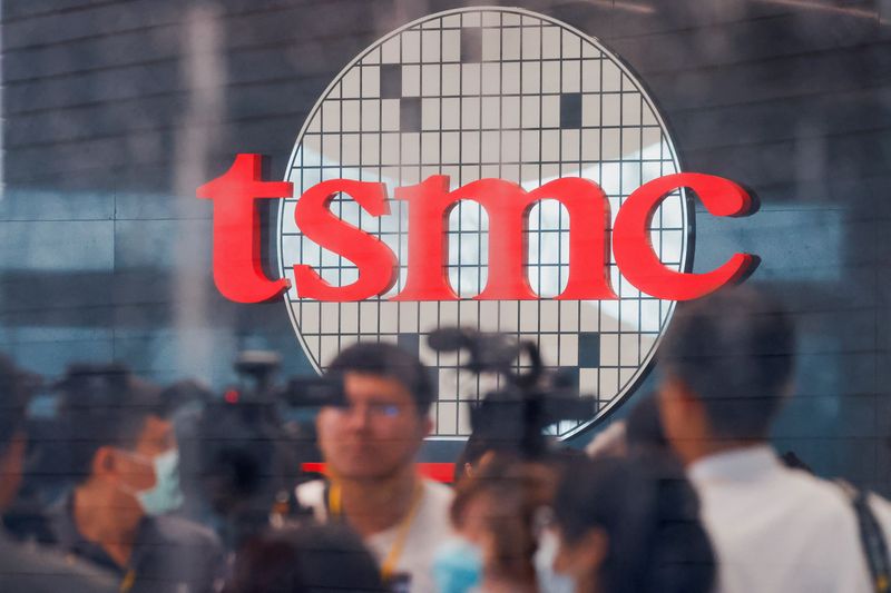
By Sam Nussey, Fanny Potkin and Miho UranakaTOKYO (Reuters) -Taiwan’s TSMC is taking a look at constructing superior packaging capability in Japan, based on two sources aware of the matter, a transfer that will add momentum to Japan’s efforts to reboot its semiconductor trade.The deliberations are at an early stage, they added, declining to be recognized as the data was not public.One choice the chipmaking large is contemplating is bringing its chip on wafer on substrate (CoWoS) packaging expertise to Japan, based on one of many sources who was briefed on the matter.CoWoS is a high-precision expertise that includes stacking chips on prime of one another, boosting processing energy whereas saving house and decreasing energy consumption.At the moment, all of TSMC’s CoWoS capability is in Taiwan.No choices on the dimensions of or the timeline for a possible funding have been made, the supply mentioned.TSMC, formally referred to as Taiwan Semiconductor Manufacturing Co, declined to remark.Demand for superior semiconductor packaging has surged globally in tandem with the bogus intelligence growth, spurring chipmakers together with TSMC, Samsung Electronics and Intel, to spice up capability.TSMC Chief Govt C.C. Wei mentioned in January that the corporate plans to double CoWos output this 12 months with additional will increase slated in 2025.On Monday, TSMC mentioned it was planning further superior packaging capability in Chiayi in southern Taiwan to answer sturdy market demand, with out giving particulars.Development of a brand new Chiayi CoWoS plant is because of begin in early Might, the island’s official Central Information Company quoted Vice Premier Cheng Wen-tsan as saying.GROWING JAPAN FOOTPRINTBuilding capability for superior packaging would prolong TSMC’s rising operations in Japan the place it has simply constructed one plant and introduced one other – each on the southern island of Kyushu, a chipmaking hub.TSMC is partnering with corporations together with Sony and Toyota with whole funding within the Japan enterprise anticipated to run to greater than $20 billion.Story continuesThe chipmaker additionally established a sophisticated packaging analysis and growth centre in Ibaraki prefecture, northeast of Tokyo in 2021.Japan is seen as properly positioned to take a bigger function in superior packaging provided that it has main semiconductor supplies and gear makers, rising funding in chip fabrication capability and a stable buyer base.Superior packaging can be welcomed in Japan which might supply the ecosystem to help it, a senior official at Japan’s trade ministry mentioned.TrendForce analyst Joanne Chiao mentioned, nonetheless, that if TSMC have been to construct superior packaging capability in Japan, she anticipated it will be restricted in scale.It was not but clear how a lot demand there can be for CoWoS packaging inside Japan and most of TSMC’s present CoWoS clients are in the USA, she added.TSMC’s plans in Japan to date have been supported by beneficiant subsidies from the Japanese authorities which – after shedding floor to South Korea and Taiwan – sees semiconductors as very important to its financial safety.That is spurred an inflow of funding from a spread of chip companies from Taiwan and elsewhere.Intel can be taking a look at establishing a sophisticated packaging analysis facility in Japan to deepen ties with native chip provide chain corporations, two separate sources aware of the matter mentioned.Intel declined to remark.Samsung is establishing a sophisticated packaging analysis facility in Yokohama, southwest of Tokyo, with authorities help.The South Korean chipmaker can be speaking to corporations in Japan and elsewhere about procuring supplies because it prepares to introduce a packaging expertise utilized by its rival SK Hynix to catch up in excessive bandwidth reminiscence chips, Reuters has reported.(Reporting by Sam Nussey, Fanny Potkin and Miho Uranaka; Further reporting by Ben Blanchard in Taipei; Modifying by Edwina Gibbs)

Unique-TSMC contemplating superior chip packaging capability in Japan, sources say

- Trending
- Comments
- Latest


